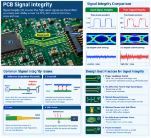
PCB signal integrity (SI), briefly saying, is could a signal be maintain with the intended voltage, timing, and waveform quality, as it passes along PCB traces.
If the waveform arriving at the receiver end and remains as “clean, timely, and correct in amplitude” as the transmitting was started, the signal integrity is considered good.
Otherwise, if the waveform suffers from distortion, delay, oscillation, or amplitude attenuation, signal integrity is not good.
As modern electronic devices evolve toward higher speeds, higher frequencies, lower voltages, and higher component densities, signal integrity has become one of the most critical challenges and concerns in PCB design.
I. What are the main issues associated with signal integrity?
1. Reflection
When a signal traveling along a trace and encounters an impedance discontinuity (such as changes in trace width, vias, connectors, or loads), a portion of the energy reflects back to the source.
This causes overshoot, undershoot, ringing, or even false triggering at the receiver.
2. Crosstalk
Traces interfere with each other through electric fields (capacitive coupling) and magnetic fields (inductive coupling). A signal transition on one trace induces noise on a neighboring trace, potentially leading to bit errors or timing jitter.
3. Ground Bounce and Power Noise
When a large number of I/O signals switch simultaneously, parasitic inductance in the return current path could cause voltage fluctuations.
This destabilizes the ground or power planes, interfering with the MCU’s normal operating.
4. Timing Issues
Flight time variations, clock skew, and setup/hold time violations.
Inconsistencies in signal arrival times can lead to data sampling errors.
5. Electromagnetic Radiation (EMI)
When high-speed signals travel across a PCB, an incomplete return path or the formation of an antenna-like structure can cause electromagnetic energy to radiate outward.
This interferes with other equipment and may prevent the electronic device from passing EMC certification.
6. Loss and Attenuation
At high frequencies, conductor resistance (skin effect) and dielectric loss may reduce signal amplitude.
This causes the eye diagram to close, making it difficult for the receiver to interpret the signal correctly.
II. Overall Impact on the PCB
Signal integrity (SI) issues are seperated alone, they affect the whole PCB and the entire electronic system, across multiple levels:
1. Functional Failure
Data errors, communication interruptions, system crashes, and abnormal resets.
In severe cases, the electronic product fails entirely and completely.
2. Reduced Timing Margins
Eye diagram closure and insufficient setup/hold times, that will prevent high-speed interfaces (such as DDR, PCIe, USB, and HDMI) to achieve expected operating rates.
The system must compromise and operate at reduced frequencies, resulting in degraded performance.
3. Compromised Electromagnetic Compatibility (EMC)
Excessive radiation and conduct emissions.
Products will be difficult and hardly pass certifications, such as FCC, CE, and CCC, which will delay the market launches.
4. Increase Power Consumption and Heat Generation
Reflections, ringing, and crosstalk, they cause additional losses.
Increase power supply noise and it leads to unstable operation of MCU or even localized overheating.
5. Increase Design Costs and Development Cycles
Signal Integrity issues exposed at late phase of development process, that often requires revisions, additional termination components, layer changes, stack-up adjustments, or even complete redesigns.
That will require additional prototyping, extend debugging times, definitely increase R&D expense and times.
6. Reduced Reliability and Lifespan
Components sustain more stress from noise, overvoltage, and overcurrent conditions.
Products may experience occasional failures that are hard to troubleshoot or diagnose.
7. Constraints on Physical PCB Design
To improve Signal Integrity, PCB design should requires:
– Controlled impedance (e.g., 50Ω single-ended, 100Ω differential);
– Continuous reference planes to avoid crossing split planes;
– Strategic planning of stack-ups and routing topologies;
– Implementation of termination, via optimization, ground guarding, and isolation techniques;
These factors influence the PCB’s layer counts, dimension, routing complexity and manufacturing cost.
III. Summary
Signal integrity is a critical concern in high-speed PCB design, it determines whether signals are transmitted correctly and also has a significant impact on system functionality, performance, EMC, power consumption, reliability, and cost.
A PCB with poor signal integrity may fail to operate reliably, even if the schematic design is flawless.
Conversely, a PCB with good signal integrity, it ensures stable, reliable, and low-noise operation under high-speed, high-density, and low-voltage conditions.
Therefore, per PCB design, signal integrity analysis(simulation, pre-layout analysis, post-simulation, and testing/verification) — is typically conducted with schematic design, layout and routing, power integrity analysis, and EMC analysis, it’s the best tactic, much better than remedial measure after the PCB has been manufactured and found out the flaws.