I. Material Selection and Compatibility
Materials directly determine the performance and reliability of PCB(printed circuit board):
– Electrical Performance Matching: Different application scenarios (high-frequency, high-speed signal transmission, etc.) have different requirements for the conductivity, insulation, and dielectric constant of materials. For example, the processing of special materials are extremely difficult, such as PTFE (polytetrafluoroethylene) and ceramic substrates.
– Processing for Special Materials: Special materials such as PTFE, metal-core PCB, and ceramic PCB, their materials require professional handling techniques, experience, equipment and processing capabilities, which might beyond the conventional manufacturers’ processes management.
– Upgraded Specifications of CCL(Copper Clad LaminatE) : For example, the PCB in NVIDIA’s Kyber rack uses a 78-layer design, M9-level copper clad laminate, and quartz fabrics, significantly increasing the amount and processing difficulty of CCL.
II. High-Density Interconnect (HDI) and Precision Processing
As the trend of electronic devices development is prefer to minimize the dimension and integrate more functionals, the manufacturing processes have to keep pace, the tracing space on a limited dimension becomes increasingly scarce. The technological challenges for high-density interconnects (HDIs) include:
– Microvia: Laser drilling requires achieving extremely small mechanical hole diameters (0.15mm) and extremely small laser holes (0.075mm), with extremely high requirements for microvia filling.
– Trace width and spacing: HDI PCBs need to achieve micron-level trace accuracy, such as trace width and spacing of only 1.2mil (approximately 0.03mm).
– Layer alignment: The alignment tolerance between layers in multilayer boards is generally controlled within 75 microns. Large-size boards are prone to misalignment due to temperature and humidity fluctuations.
– Blind and buried vias: Complex processes such as HDI blind and buried vias and back-drilling technology require extremely high precision for equipment.
III. Multilayer Board Lamination Process
The lamination process for multilayer PCBs (10-20 layers or more) is a core challenge:
– Sliding and delamination: When multilayer boards are overlapped and laminated with prepreg, defects such as sliding, delamination, resin gaps, and residual air bubbles are prone to occur.
– Expansion and contraction control: Multilayer structures cause inconsistencies between expansion and contraction control, and dimensional compensation. Insulation between thin layers can easily lead to failures of reliability test.
– Design for stackup: A reasonable laminating scheme is needed in advance for multi-layer board, developed by comprehensively consideration and factors, such as heat resistance, pressure resistance, adhesive content, and dielectric thickness.
IV. Drilling Quality
– Hole wall defects: Manifested as uneven hole walls or residue, affecting electrical connections.
High TG, high speed, high frequency, and thick copper PCBs could increase roughness of drill bit, burrs, and the difficulty of decontamination.
– Drill bit wear: Repeatly drilling at overlapped solder pads, can easily break the drill bit and cause hole damage.
– Deburring and cleaning: Deburring and ultrasonic cleaning are required after drilling, to ensure smooth and clean hole walls.
V. Reflow Soldering and Surface Treatment
– Soldering process control: temperature and time of reflow soldering, need to be precisely controlled, to prevent solder joint defects and trace breaks, caused by oxidation and thermal stress.
– Pad lifting: Insufficient pad adhesion might lead to pad lifting during high-temperature reflow soldering process.
Surface treatment technologies, such as chemical nickel-gold plating, could enhance the adhesion of solder pads.
– Surface Treatment Defects: Issues such as uneven plating thickness and poor solderability, that require optimization of plating solutions, such as composition and temperature control.
VI. Signal Integrity and Electromagnetic Compatibility (EMC/EMI)
– Signal Integrity: Per high-frequency/high-speed signal transmission PCB, requires attention to impedance matching, crosstalk control, and inter-layer interference.
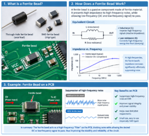
– Electromagnetic Compatibility: Appropriate shielding and filtering components are needed, to reduce electromagnetic radiation and improve anti-interference capabilities.
– Power Supply and Signal Separation: Power supply loops and signal loops must be isolated, to prevent power noise and affecting signal transmission.
VII. Thermal Management
– With the power consumption increasing from electronic components, heat dissipation has become a core concern and critical challenge.
– Reasonable layout of heat dissipation structures, and the apply materials such as heat sinks/thermal paste, to ensure the heat-dissipating of PCBs.
– Thermal management in telecommunication equipment now faces multiple challenges, including high power density, heat dissipation and heat dissipation channels.
VIII. Quality Control and Yield
– Solder Mask Defects: Cracks, blistering, or peeling, that reduce protection performance on PCB. Temperature and time of ink curing should be rigorously controlled.
– Short circuit: Caused by conductive particle, contamination or improper design, requiring rigorous process control.
– AOI inspection: Fine-trace which carries signals on inner layers, in a high probability of being missed by AOI, resulting in wrinkles, poor exposure, and easy for curling, leading to high cost when the PCBs are defective.
– Ultra-high multilayer PCB yield: For example, 78 layers PCBs in yield control, the impedance consistency, heat dissipation, etc, are far more difficult to maintain the quality than conventional PCBs.
Kyrid has been manufacturing PCB for over a decade, professional and well experienced for material order, stock, transportation, process and quality control. Whereever you need PCBs, Kyrid is gladly to deliver high-quality PCB with competitive price!