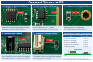
Component clearances, refer to the minimum physical distance that must be maintained between the components on PCB.
It’s core purpose is to ensure the components on PCB have enough space surrounding them, won’t affect each other and sequence processes&opteration, such as SMT/DIP assembly and repair work.
Typical Clearance Values
The clearances depend on component type, size, and manufacturer’s capabilities.
Here below are common industry guidelines:
| Component Type | Recommended Minimum Clearance | Purpose / Notes |
|---|---|---|
| Small Components (<0603) — Resistors & Capacitors | ≥ 0.15 mm | Prevents component-to-component interference and solder bridging |
| Standard SMT Packages (0402–1206) | ≥ 1.0 mm | Provides sufficient space for SMT assembly and inspection |
| ICs (QFP, BGA) | ≥ 3.0 mm | Allows adequate space for SMT assembly, inspection, and rework |
| Connectors, Crystals & Electrolytic Capacitors | ≥ 0.5 mm | Maintain additional clearance for assembly; mating clearance must also be considered |
| BGA Microprocessor | ≥ 1.0 mm | Provides adequate spacing around the BGA package for assembly and rework |
| Heat-Generating vs. Heat-Sensitive Components | ≥ 5.0 mm | Reduces thermal interference and helps protect temperature-sensitive components |
| Through-Hole Components | > 2.0–3.0 mm | Recommended for wave soldering and manual soldering access |
Key Factors Influencing Clearance
– Manufacturing (DFM): Stencils require enough space to print solder paste properly, and Pick-and-place nozzles need space to descend and mount components on solder pads. Insufficient clearance might cause bridging or assembly defects.
– Rework & Repair: Space is needed around components, especially ICs, to allow soldering irons or hot-air tools to work on the pads when need to remove and replace the components.
– Thermal Management: Heat-generating components (like power inductors, IGBT, Transistors) should keep distance from heat-sensitive parts, thus to prevent performance drift.
– Electrical Safety: For high-voltage designs, component spacing may need to be increased to meet specific clearance requirements (e.g., per IPC-2221).
Setting Clearances in EDA Software
In tools like Altium Designer, this is managed through the Component Clearance design rule.
You can find it under Design → Rules → Placement → Component Clearance.
Within the rule, you can set the Minimum Horizontal Clearance and choose a check mode (e.g., Quick Check for speed or MultiLayer Check for precision using 3D models).
Manufacturer-Specific Rules
Always verify the manufacturer’s specific design rules.
For example, Kyrid specifies the default as 0.25 mm, but 0.15 mm for smaller components below package 0603, and 1.0 mm for BGAs. And Kyrid also recommends 10 mil (0.254 mm) of courtyard clearance at least.
Do you want to learn more acknowledges about PCB fabrication? Leave a message below for what subjects you like and Kyrid team will respond with a good article!