DFM, is shorted from Design for Manufacturability, it essentially means considerations below, during the PCB design phase:
– Process limitations
– Production constraints
– Capabilities of subsequent manufacturing and assembly
It ensures that the PCB is not merely designed, but can be manufactured reliably, efficiently, and cost-effectively as well.
A PCB may work perfectly in a simulation but still be difficult or expensive to manufacture. DFM checks the design before production to identify those problems.
It acts as a bridge, transporting design intention to physical manufacturing outcomes.
Why is DFM so important?
Many engineers believe that once the designs passed the EDA software’s Design Rule Check (DRC), that means the design is ready for production.
However, while DRC verifies electrical rules, DFM verifies physical manufacturing limits and constraints.
Neglecting DFM might lead to serious consequences:
1. Skyrocketing costs:
Pushing design parameters to the limits(maximum or minimum) of a factory’s process capabilities (such as using extremely small vias) might be technically feasible, but it leads to higher rates of drill bit breakage and increase defect rates — costs that will eventually pass on to you in the price.
2. Delivery delays:
If a factory discovers the design is unmanufacturable, they issue Engineering Queries (EQs) and back-and-forth communication with the designer will take additional times, this process commonmly take 24 to 48 hours or even longer.
3. Reliability risks:
A PCB board might pass factory’s test like flying probe and fixture testing, but insufficient annular ring width could cause the pad to peel away or break from the substrate after several thermal cycles — a failure that might only expose after months later.
Core DFM Checklist: What should PCB design engineers focus on?
When performing DFM analysis, there are several aspects of physical conflict, where errors are most likely to occur, that requires careful verification:
1. Trace width and spacing
– Trace width/spacing:
This is the most fundamental DFM checkpoints.
Designs must meet the manufacturer’s minimum specifications & constraints for trace width and spacing, to avoid the risk of short circuits or open circuits.
For example, standard manufacturing capacities might require a 5-mil trace width and spacing.
– Copper slivers:
When traces form an acute angle (less than 90 degrees), etchant can be trapped in the corner, causing over-etching that might “sever” the trace. Although modern processes have been improved, these angles should still be avoided.
– Drill-to-copper clearance:
Mechanical drilling involves alignment tolerances.
It is recommended to maintain a minimum clearance of 8 mils, to prevent traces from being severed due to drill misalignment.
2. Vias and Pads
– Annular Ring:
This refers to the copper ring remaining between the hole wall and the outer edge of the pad after drilling.
If the ring width is insufficient, the connection between the via and the trace is prone to breaking. This is a common issue during inner-layer DFM checks.
– Via-in-Pad:
While placing a via directly on an SMD pad could save space, but failing to use resin-plugging will cause solder paste to flow away during reflow-soldering, resulting in poor solder joints (cold joints).
Unless a specific process requires it, this approach should generally be avoided.
3. Solder Mask and Silkscreen
– Solder Mask Opening:
Due to printing tolerances, the solder mask opening must be 2–4 mils larger than the pad on each side, otherwise, mask ink encroaching on the pad edge might cause soldering defects.
– Solder Mask Dam:
A sufficiently wide solder mask dam must be maintained between fine-pitch IC pins, to prevent short circuit during reflow soldering.
– Silkscreen/Legend Clarity:
Silkscreen/legend must never overlap with pads.
Even if the manufacturer automatically removes the overlapping legends, it may result in missing characters in reference designators, losing the designator reference for future works and identifications.
4. PCB Panelization and Board Outline
– Process Edge and Fiducial Holes/Marks:
To ensure to transport PCB through SMT lines stably, process edges are usually added on to the panel, along with fiducial marks (reference points) for vision alignment.
– Copper Balancing:
If the top side of the board has significant copper coverage while the bottom has very little, severe internal stress will accelerate and enhance during lamination, causing the board to warp.
Excessive warping rate could reduce SMT assembly yields.
Difference Between DFM and DFA
You may hear the terms DFM and DFA being bring up together, simply differenatation: DFM ensures the bare PCB can be well manufactured, while DFA ensures components can be successfully mounted onto PCB (PCB Assembly).
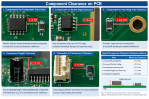
DFM focuses on the PCB fabrication process, where DFA focuses on the assembly process — such as component spacing and whether placement machine nozzles have sufficient clearance to access specific areas.
How to Effectively Implement DFM?
1. Integrate DFM rules at earlier phase:
A best practice is to input the manufacturer’s process capabilities—such as minimum trace width, spacing, and hole size—into the EDA software’s rule manager during the layout phase. This prevents violations at the source rather than relying on checks after the design is complete.
2. Leverage professional tools:
Beyond the built-in rules in EDA software, many PCB manufacturers offer free online DFM analysis tools, that automatically check design files and notice potential issues before start of production.
3. Consult the manufacturer:
Manufacturing capabilities are diffenent between factories. Before start the designing process of high-density or complex boards, it would be better to obtain the specific capability parameters and production constraints from the factory and base the design on those specifications.
Summary:
DFM helps to achieve:
Better manufacturability → less defects → prevent rework → low cost → reliable production → good quality, good price
For example, if two PCB traces are designed too close, it may difficult to etch them, and also easy to cause shorts and open circuits. DFM check could identify the potential risk and alert to revise, before the design proceed to production.
PCB DFM is a design mindset and philosophy that with certain standards, to proceed design process and prevent to revise or even mistakes in future. It requires PCB design engineers to keep circuit design principles in mind and also the capacities and process of the manufacturing — such as drill bits, etching solutions, and pick-and-place nozzles.