PCB test points are solder pads and vias on the circuit board, exposed on the surface, without coverage like solder mask or silkscreen, specially designed for electrical testing.
The core purpose of test points is to reserve reliable physical connections for automated testing (especially ICT online testing) and manual debugging/repairing, to complete the inspection of various performance of the circuit boards, and quickly detect whether the components have soldering issues such as short circuit, open circuit, absence of components and parameter deviation.
1. The test points mainly serve two core purpose: automated testing (ICT) and manual debugging/repairing:
– ICT testing: When going through mass production, ICT could test and detect the circuits through test points systematically and automatically, protecting components.
Nowadays, manufacturers mount a large number of components on PCB by SMT (surface mount) technologies, and the components are very fragile, if contact the components directly with the test probe, that might damage the components or their solder joints, causing physical damage.
The test points provide independent connections and also avoid connection problems such as poor connection caused by flux residues that cover up the solder pads or leads, improve stability of testing and support the nail bed of automated equipment such as ICT (in-circuit testing), to contact hundreds or even thousands of points at the same time.
The test point also prevent the probe to damage fragile components directly, pierce the flux residue on the solder surface, to ensure reliable electrical contact. It could complete the testing of electrical performance and soldering quality, inspection of resistors, capacitors, IC and other components on the board just in 1-2 minutes.
– Debugging and repairing: When the circuit board is on the R&D stage or repairing, the test points could assist troubleshotting by oscilloscope and multimeter, to measure signals such as waveforms, electrical current and voltages through them, quickly pindown the failed or defective circuit and specific components, very convenient and helpful for troubleshooting.
*Reminder: When measuring signals, the test points should be placed at the signal receiving end (such as the chip pin), not the transmitting end. Otherwise, distorted waveforms may be measured due to signal reflection, leading to misjudgment.
2. Design logic of test points:
The layout logic of test points is essentially the implementation of Design for Testability (DFT), which needs to take into consideration of physical accessibility, electrical reliability and fixture feasibility.
In order to make sure the test points could work reliably, the size, spacing and location of the test points must match the physical capabilities of the test fixture (bed of nails), otherwise, the fixture cannot be made at all or might easily lead to damage. A series of rules and regulations need to be concerned during design process:
PCB Test Point Design Requirements
| No. | Design Parameter | Recommended Requirement | Design Purpose / Notes |
|---|---|---|---|
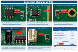
| 1 | Solder Pad Size | Ø0.8–1.2 mm preferred | Pads that are too small may cause probe drift or unstable contact. Pads that are too large consume more PCB space. |
| 2 | Center-to-Center Distance | ≥1.27 mm (50 mil); 2.54 mm (100 mil) preferred | Sufficient spacing is required to prevent probe sheaths from interfering with each other. |
| 3 | Distance to PCB Edge | ≥5 mm from the board edge | Prevents potential damage to test points during depanelization and provides sufficient fixture clearance. |
| 4 | Distance from Components | ≥3 mm from components | Provides sufficient space for probe access and prevents physical interference. |
| 5 | Distance from Tall Components | ≥5 mm from tall components such as electrolytic capacitors and connectors | Ensures sufficient vertical space for the probe to press down and prevents physical collision with components. |
| 6 | Surface Finish / Exposure | Test points must be exposed and must not be covered by solder mask or silkscreen. | Provides reliable electrical and mechanical contact between the probe and test point. |
| 7 | Recommended Surface Finish | HASL or ENIG | Both finishes are recommended for reliable probe contact and test-point durability. |
| 8 | Test Point Layout | Place test points on the same side of the PCB whenever possible. | Reduces test fixture complexity and manufacturing cost. |
| 9 | Test Point Distribution | Distribute test points evenly across the PCB. | Avoids concentrated probe pressure, uneven mechanical stress, PCB bending, and warpage. |
Note: Any deviation from these requirements should be reviewed and approved by the PCB design and test-fixture engineering teams.
3. Network coverage and electrical requirements:
1) In theory, each electrical network (Net) on the circuit board, should have at least one test point, to achieve 100% coverage and ensure that every key electrical trace&joint can be tested;
2) For key networks such as power supply, clock, reset, etc., it is best to have 2 test points, to improve test coverage;
3) For packages such as BGA that cannot contact the pins directly, the signal needs to be led out through vias or pads nearby as a test point;
4) Power and ground pins of each IC must have test points and positioned as close as possible. It is recommended to have more than 2 test points on the power supply network, to monitor voltage drops at different locations;
5) Electrical isolation: The test point itself might affect signal integrity, to avoid such potentialality, have to leave sufficient distance from high-frequency signal traces.
4. Precautions for actual testing:
Pay attention to the details during the actual testing process, that will help to avoid mistesting or fixture damage.
1) Solder mask and contaminant
This is the most common and most neglective issues. The test point must be fully exposed through solder mask opening, to ensure that the solder pad could be well contacted with testing probes. Any solder mask or silk screen that covered the test points, in high risk to cause poor contact and lead to unvalid measurement and wrong results. Before testing, it is necessary to ensure that the surface of the test point is free of insulating contaminants such as flux residue as well.
2) Component height
During the testing process, it is necessary to pay attention to the height of large-size components, such as aluminum electrolytic capacitors, connectors, large transformers, IGBT, etc., and the gap between them and fixture. Especially after DIP&wave soldering process, the components might not be assembled on the correct height, floating with a little bit higher, then cause physical damages by pressing or even collision;
5. Trends and Limitations
1) Challenges of high density and double-sided testing
With the trend of miniaturization and intensification of PCB, the space on PCB is increasingly getting tighter. Alternative solutions can be considered to reduce the number of physical test points, such as applying JTAG to test digital IC interconnections, or technologies such as TestJet to test the electrical connections of BGA and other component pins.
If double-sided testing is necessary, the test points on the top and bottom layers need to be staggered in layout, otherwise the fixture probes may conflict with each other and cause a short.
2) Special dealing of high-value and high-density components
For components with covered, invisible pins, such as BGA, the solder joints beneath them cannot be directly contacted, so we can consider to positioning test points on the periphral circuit, for each critical power and signal network, or on the bottom side of the PCB, so that ICT can contact them and test are they with potential issues.
Summary and suggestions
On the design stage, engineers shall communicate with PCB test process engineers and fixture suppliers in advance, to clarify the production constraints and testing process.
The key concerns are as follow:
1) Confirm the supplier’s capabilities: Before layout, be sure to the minimum diameter of probe, minimum test point spacing and other parameters from the fixture manufacturer;
2) Strictly follow the specifications: use basic specifications such as “opening, 5mm distance away from the edge, avoid big-size components, and evenly deploy the test points” as design rules;
3) Make good use of alternative solutions: When space on PCB is insufficient, evaluate to apply JTAG, TestJet and other solutions, that could reduce reliance on test points;
Besides PCB fabrication and manufacture test points well, Kyrid also provide ICT testing and customize testing fixtures with nail bed, to test each PCB and PCBA and confirm working well before delivery to customers. If you are interested and in need of our service, please feel free to reach out.